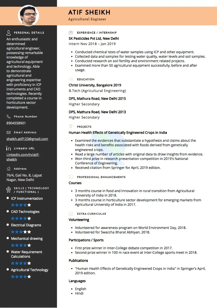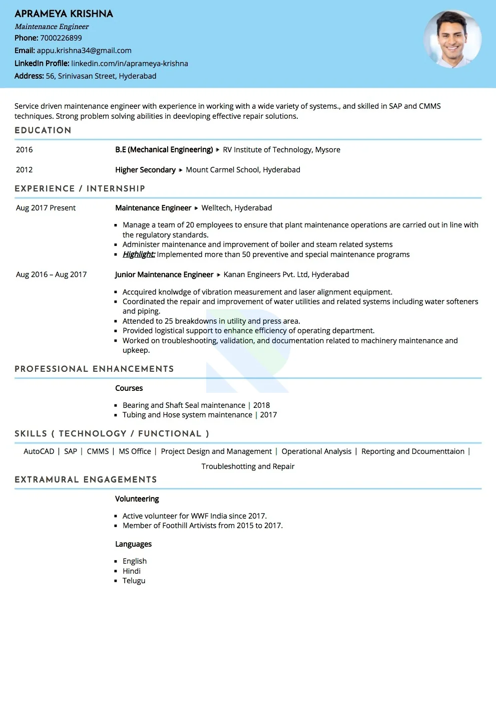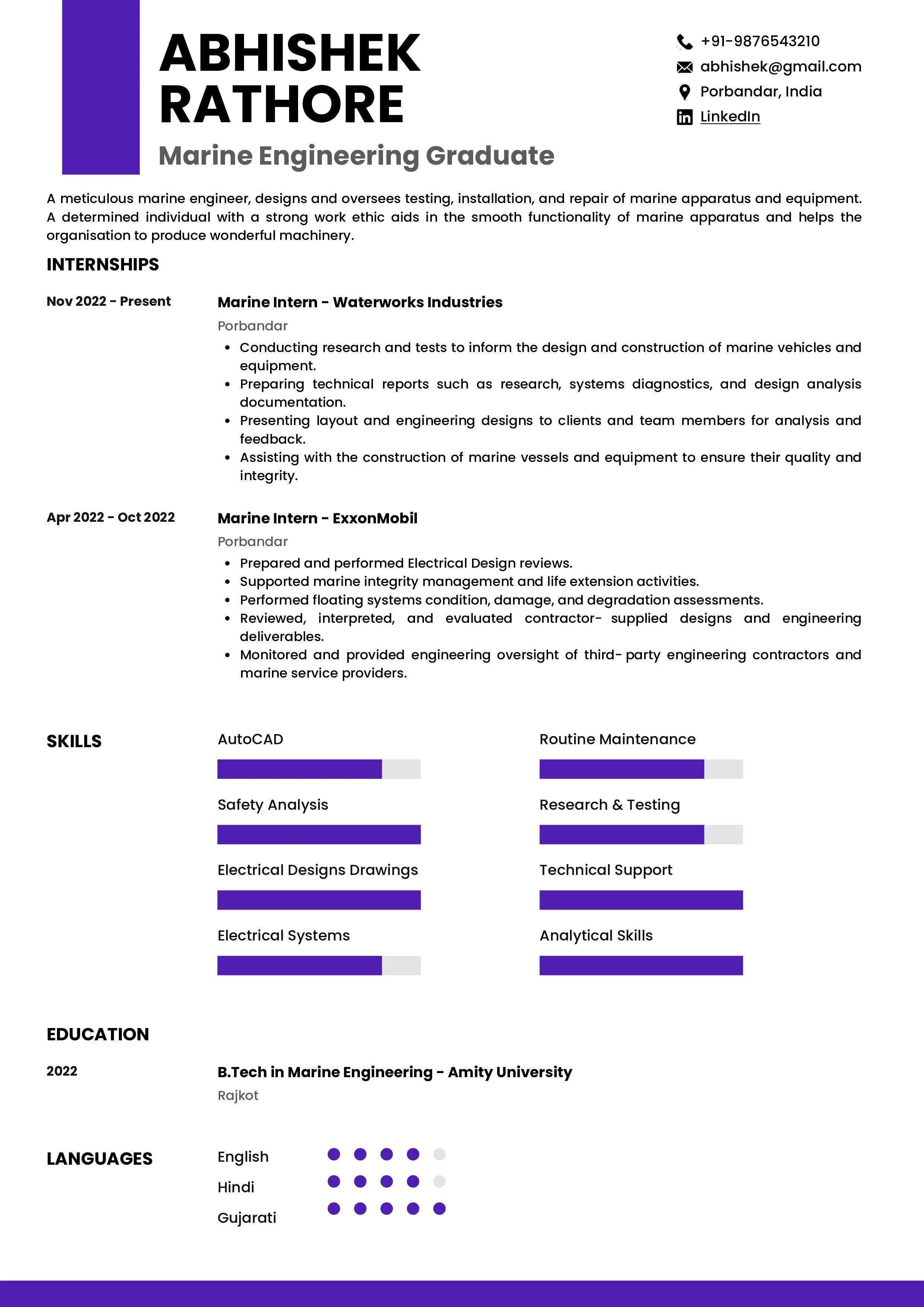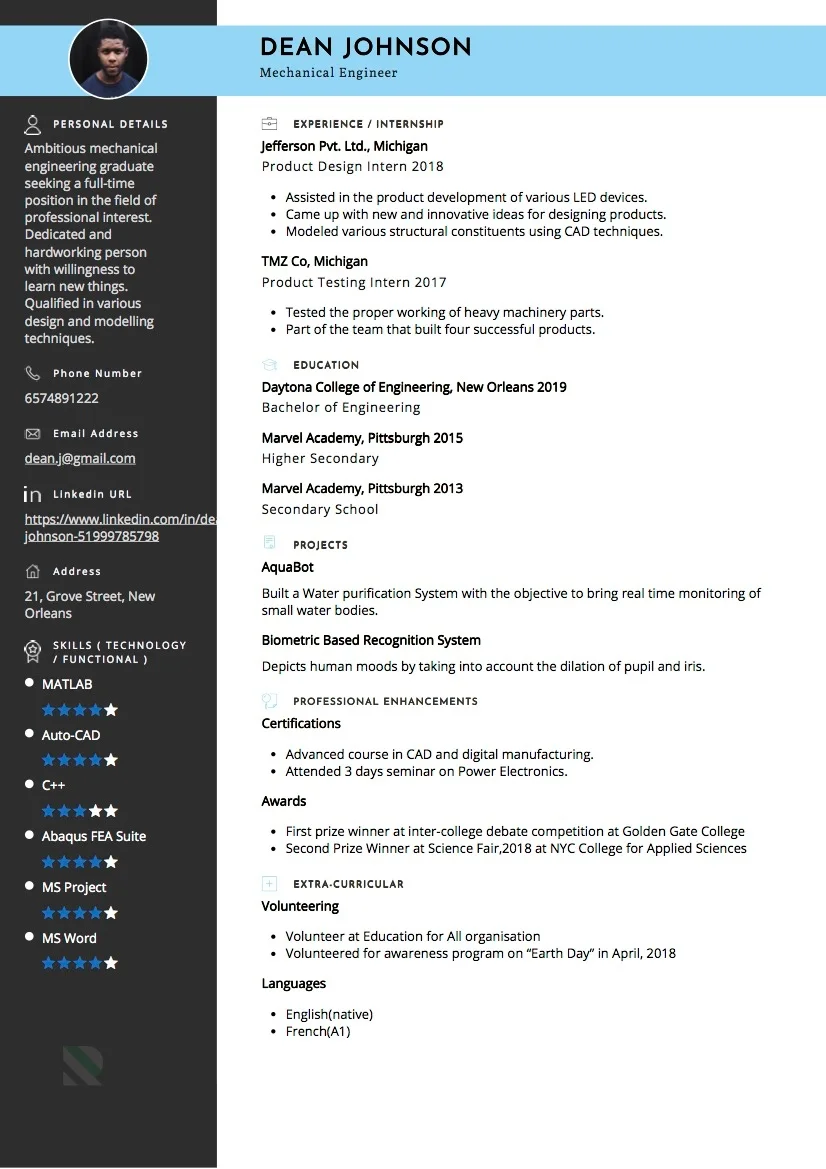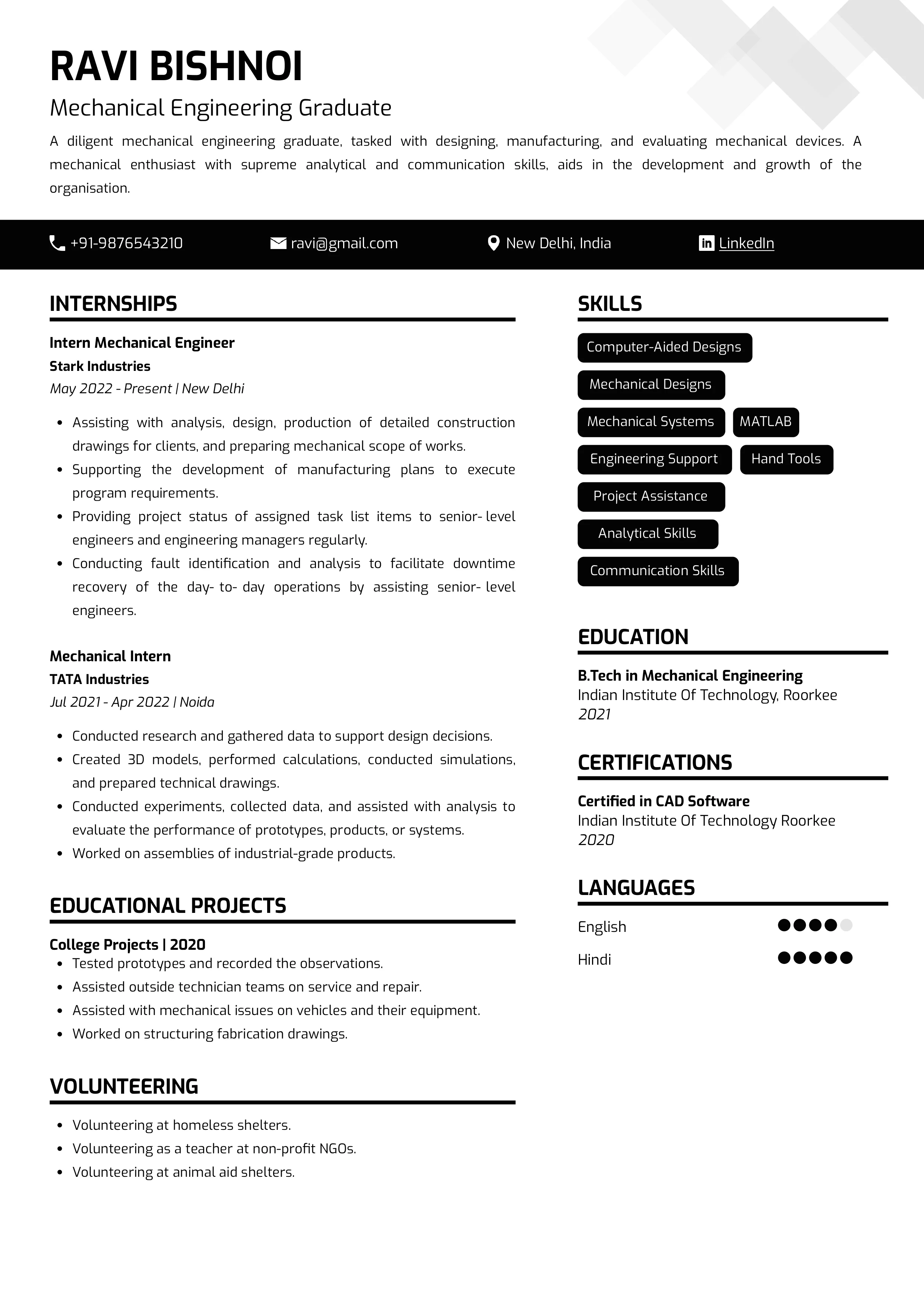

 2461
2461
Resume Skills and Keywords for a Semiconductor Engineer
LONG DESCRIPTION
A Semiconductor Engineer plays a crucial role in the development of cutting-edge electronic systems by designing, optimising, and validating integrated circuits and semiconductor devices. They are involved throughout the product development lifecycle—from architecture definition and circuit design to fabrication support, testing, and yield improvement. Leveraging expertise in VLSI design, semiconductor physics, and EDA tools, they translate complex functional requirements into high-performance, low-power chip solutions. Working closely with cross-functional teams, including design verification engineers, process engineers, and system architects, Semiconductor Engineers ensure that the final product meets stringent specifications for speed, efficiency, and reliability.
Skills required for a Semiconductor Engineer role:
- CMOS technology
- VLSI Design
- Python
- Cadence Design Systems
- Mentor Graphics
- Layout and Circuit Simulation
- Testing and Validation
- Wafer Handling
- Synopsys tools
What recruiters look for in a Semiconductor Engineer's resume:
- Bachelor’s or Master’s degree in Electronics & Communication, Electrical Engineering, VLSI, or a related field.
- Strong foundation in semiconductor device physics, circuit theory, and microelectronics.
- Hands-on experience with VLSI design, RTL coding (Verilog/VHDL), and SoC development.
- Proficiency in using industry-standard EDA tools such as Cadence, Synopsys, Mentor Graphics, or LTSpice.
- Knowledge of digital and analog circuit design, simulation, and layout verification techniques.
- Experience with semiconductor fabrication processes, DRC/LVS checks, and cleanroom protocols is a plus.
- Familiarity with scripting languages (e.g., Python, TCL, Shell) for automation and design validation.
- Understanding of low-power design methodologies, signal integrity, and timing analysis (STA).
What can make your Semiconductor Engineer resume stand out:
A strong summary that demonstrates your skills, experience and background in engineering
- A precise Semiconductor Engineer with a strong foundation in VLSI design, semiconductor device physics, and digital/analogue circuit simulation. Recently graduated in Electronics and Communication Engineering, with hands-on experience in academic projects using industry-standard EDA tools like Cadence, Synopsys, and LTspice. Dedicated to designing innovative and energy-efficient chip solutions for next-generation electronic systems.
Targeted job description
- Lead the design, development, and optimisation of complex semiconductor devices, including digital, analog, or mixed-signal integrated circuits (ICs).
- Drive end-to-end VLSI/ASIC/FPGA design flows, from architecture definition and RTL coding to synthesis, place & route, and timing closure.
- Utilise industry-standard EDA tools (Cadence, Synopsys, Mentor Graphics) for circuit simulation, verification (DRC/LVS), and physical design.
- Collaborate with cross-functional teams, including design verification, packaging, process engineering, and product teams, to ensure successful tape-out and silicon validation.
- Perform advanced analysis on power, performance, and area (PPA), and implement low-power and high-speed design techniques.
Related academic background
- B.Tech in Electronics and Communication Engineering at Indian Institute Of Science, Bangalore | 2020
Sample Resume of a Semiconductor Engineer in Text Format
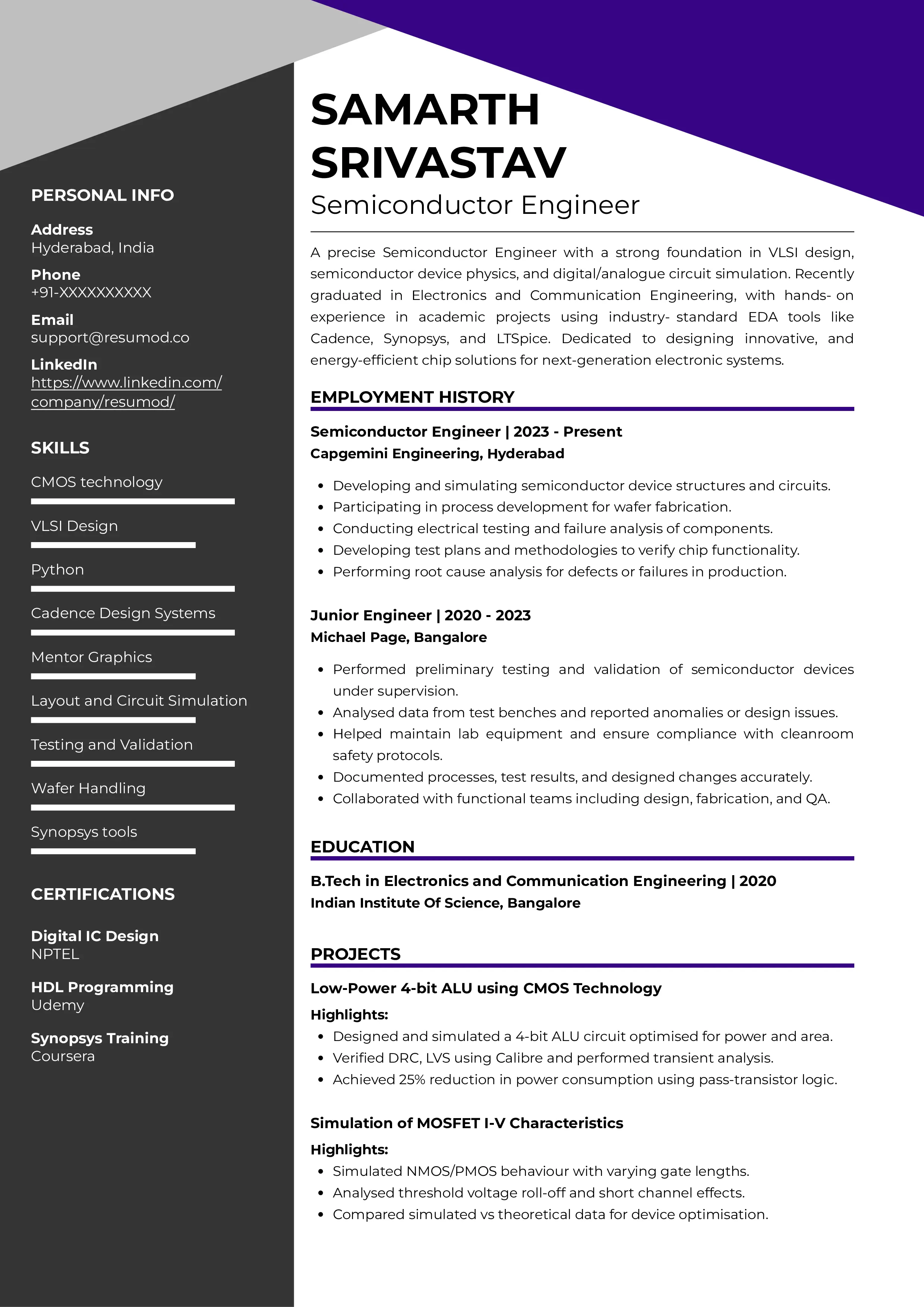
SAMARTH SRIVASTAV
Semiconductor Engineer
+91-XXXXXXXXXX | support@resumod.co |Hyderabad, India
SUMMARY
A precise Semiconductor Engineer with a strong foundation in VLSI design, semiconductor device physics, and digital/analogue circuit simulation. Recently graduated in Electronics and Communication Engineering, with hands-on experience in academic projects using industry-standard EDA tools like Cadence, Synopsys, and LTspice. Dedicated to designing innovative, and energy-efficient chip solutions for next-generation electronic systems.
EMPLOYMENT HISTORY
Semiconductor Engineer at Capgemini Engineering from 2023 - Present, Hyderabad
- Developing and simulating semiconductor device structures and circuits.
- Participating in process development for wafer fabrication.
- Conducting electrical testing and failure analysis of components.
- Developing test plans and methodologies to verify chip functionality.
- Performing root cause analysis for defects or failures in production.
Junior Engineer at Michael Page 2020 - 2023, Bangalore
- Performed preliminary testing and validation of semiconductor devices under supervision.
- Analysed data from test benches and reported anomalies or design issues.
- Helped maintain lab equipment and ensure compliance with cleanroom safety protocols.
- Documented processes, test results, and designed changes accurately.
- Collaborated with functional teams, including design, fabrication, and QA.
PROJECT
Low-Power 4-bit ALU using CMOS Technology
Highlights:
- Designed and simulated a 4-bit ALU circuit optimised for power and area.
- Verified DRC, LVS using Calibre and performed transient analysis.
- Achieved 25% reduction in power consumption using pass-transistor logic.
Simulation of MOSFET I-V Characteristics
Highlights:
- Simulated NMOS/PMOS behaviour with varying gate lengths.
- Analysed threshold voltage roll-off and short channel effects.
- Compared simulated vs theoretical data for device optimisation.
CERTIFICATIONS
- Digital IC Design at NPTEL
- HDL Programming at Udemy
- Synopsys Training at Coursera
EDUCATION
- B.Tech in Electronics and Communication Engineering at Indian Institute Of Science, Bangalore | 2020
SKILLS
CMOS technology | VLSI Design | Python | Cadence Design Systems | Mentor Graphics | Layout and Circuit Simulation | Testing and Validation | Wafer Handling | Synopsys tools
LANGUAGES
English
Hindi